

Electronic computer-aided design (ECAD) is typically used to design and develop electronic systems. Although the acronym is a mere letter away from “CAD”, there’s actually more to the story than appending the word “electronic” to “computer-aided design”. So, what is ECAD and why is it used in finite element analysis (FEA)?
Computer-Aided Design (CAD)
Let’s begin by discussing CAD. An engineer creates a design in 2D or 3D, where data describing the different dimensions’ positions in space are available in CAD files. Previously, these drawings gave great insight into the design of a part or assembly, and the dimensions would be manually read by the engineers building the desired product.
Today, CAD files can also be complemented by further data, such as descriptions of the material property of a part or its tolerances. CAD files can be automatically read by tools that need to work with the designs, such as the machines in the manufacturing process or the software that run FEA.
Electronic Computer-Aided Design (ECAD)
While CAD is usually used for designing a specific part or an assembly, ECAD is used to design an entire system of many components connected to each other, usually by electric circuits — like the circuit board in your computer. The intricacies of these types of designs are often quite complex for a CAD software to handle in an effective way. Looking at a typical circuit board, you can see that it is quite complex. However, if you look from the side, you can see that most of the components making up the circuit board are quite simple.
Electrical engineers have found that it is a lot simpler to design their integrated circuits (ICs) in 2D, where all of the complexity of positional data can be effectively evaluated and assessed. This dimensional data is then incorporated with extra data, such as the height of the circuit board layers and their material properties, in an ECAD file as metadata. ECAD files work perfectly for the manufacturing industry, as most ICs are produced by depositing metal and oxide layers through “masks”. The 2D data is basically the layout of the mask, while the ECAD file’s metadata instructs the manufacturing process on the material type and amount of material to be deposited.
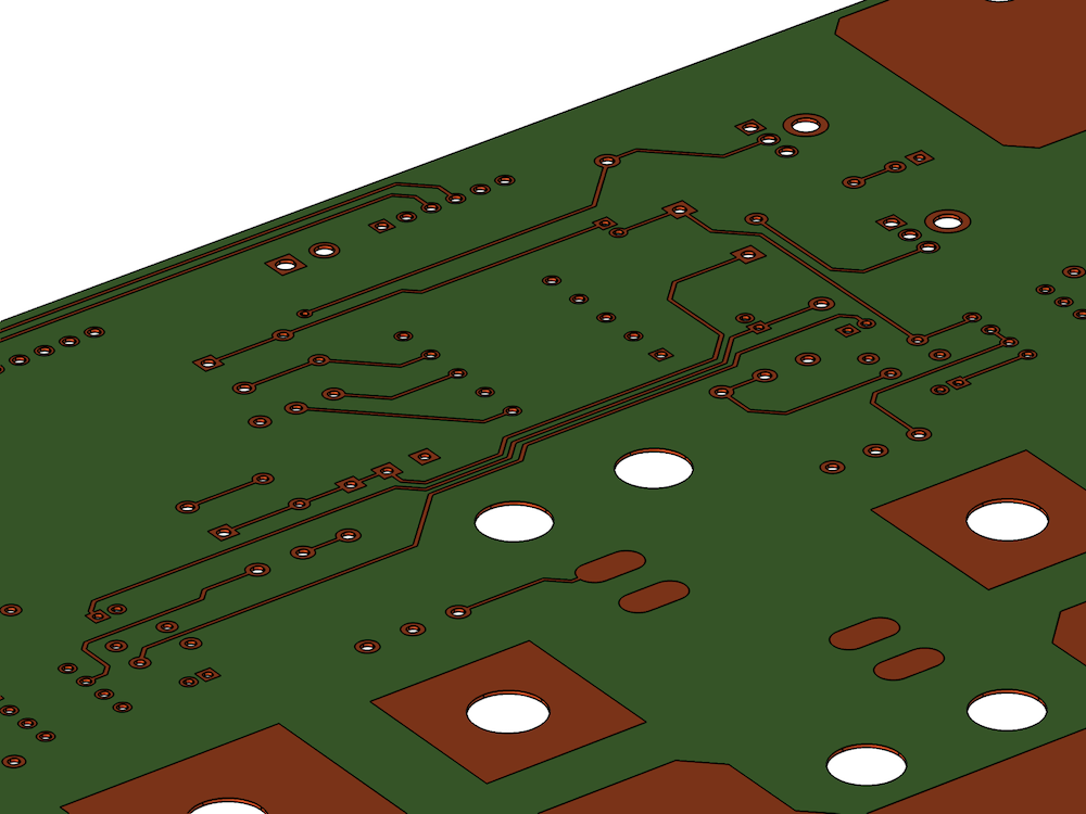
Example of a two-layer PCB geometry. The file is provided through the courtesy of Hypertherm, Inc., Hanover, NH, USA.
Moving directly from ECAD to manufacturing is becoming less viable as IC designs are customized, become smaller, and require minimal material waste. As these designs are optimized, the components making up electrical systems need to be analyzed to their established behavior within the system (such as the effects of Joule heating) as well as to external factors (i.e., how to effectively cool them). This is where simulation, such as FEA, comes into the picture. With FEA, the separate components of an IC can be tested before the final design is submitted for manufacture.
Working with ECAD and FEA
Reading ECAD files for FEA requires building 3D objects from 2D data and the accompanying metadata. This capability is available in the COMSOL Multiphysics® software with the add-on AC/DC Module, MEMS Module, and RF Module. These products are applicable for modeling the electromagnetic (and, with the MEMS Module, structural) behavior of IC components.
Next Steps
Contact us to learn more about the capabilities of COMSOL Multiphysics for FEA and ECAD and to evaluate the software.


Comments (0)