Simulation of ZnO/Si nanowires p-n Heterojunction Microarrays Diode based Gas Sensor
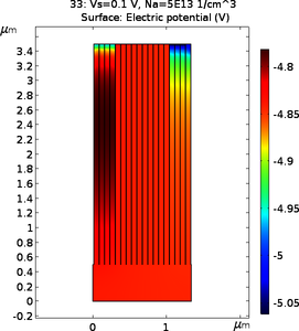
In recent year gas sensors are commercially available for use in healthcare such as exhaled breath analysis in addition to hazardous gas monitoring as new vistas for technological application. In this work we first fabricated the vertically aligned Si NW arrays experimentally and simulated the I-V data and carrier concentration of vertically aligned NWs arrays which is well agreement with experimental data. Secondly then we fabricated a ZnO/Silicon nanowires (ZnO/Si NWs) based p-n heterojunction diode which detect Nitric Oxide (NO) gas at least down to 0.5ppm (with dry N2 as the ambience gas). The device has a layer of ZnO making hetero-structure with Si NWs. The top layer of ZnO takes part in electrical current conduction. The Si NWs also has an all-round layer of ZnO that also acts as “chemical sensing gate” to modulate the depletion layer on the surface of the NW. We make a physical model based on p-n heterojunction with analysis of cross-sectional electron microscopy and line energy dispersive spectroscopy. The comparison of the simulation results with the experiment identifies the materials parameters that enhance the device response. The characteristics values of the parameters for the best fits obtained from the simulation and it can be seen that all the parameters undergo change in the electrical model and this leads to enhancement of current in the device on gas exposure. The values of p-n junction reverse saturation current (I0) increases from 5.35 x 10⁻⁹ to nearly 10-8 A an enhancement of about 49%. The resistance of the ZnO top layer film (RA) also reduces by 39%. However, the largest enhancement in the device current are contributed by drops in resistances RB and RC (42% and 52% respectively) which comes from ZnO coating around the NWs. (Note: The electrical model analysis is based on finite number of resistors and p-n junctions which are meant to capture the essential physical process. In real device there are larger number of resistors and p-n junctions. Thus the quantification of parameters from the model that we obtained from finite number of circuit elements will be treated as suggestive than rigorous). The main inference from the simulation is that the observed high performances of the sensor device depends on change in resistances of the constituents as well change in the reverse saturation current at the ZnO/p-Si NW p-n junction.